PVsyst is a software package for modeling complete photovoltaic systems including PV modules, inverters, energy storage, and electrical connection components. PVsyst employs a single diode module model with the following ancillary equations. Note that here we use $$I_L$$ and $$\alpha_{lsc}$$ to denote the light current, absorbed irradiance and temperature coefficient of $$_{sc}$$, respectively, whereas in the PVsyst User’s Guide, $$I_{PH}$$, $$G$$, and $$\mu_{lsc}$$ are used for these quantities.
$${I_L} = {S \over {{S_{ref}}}} \left[ {{I_{L,ref}} + {\alpha_{lsc}} \left( {{T_c} – {T_{ref}}} \right)} \right] \qquad$$
$${I_0} = {I_{0,ref}} \left( \frac{T_c}{T_{c,ref}} \right)^3 \exp \left[ \frac{q E_g}{nk} \left( \frac{1} {T_{ref}} – \frac{1}{T} \right) \right] \qquad$$
In the PVsyst User’s Guide, $$\gamma$$ is used to denote the diode quality (ideality) factor where we use $$n$$. The bandgap voltage term $$E_{g}$$ is regarded as constant in PVsyst and values are provided for various technologies (e.g., 1.12 eV for cSi) in the PVsyst User’s Guide.
$$R_s = \rm constant \qquad$$
$$R_{sh}\left( S \right)= R_{sh,base}+\left(R_{sh,0} – R_{sh,base} \right)\exp\left(-R_{sh,exp}\left(\frac{S}{S_{ref}}\right)\right)$$
$$R_{sh,base} = \max\left\{\left(\frac{R_{sh,ref}-R_{sh,0}\exp\left(-R_{sh,exp}\right)}{1-\exp \left(-R_{sh,exp} \right )} \right ), 0 \right\}$$
The equation for $$R_{sh,base}$$ is published in [1] and was confirmed through discussions between its authors and PVsyst.
In the PVsyst User’s Guide, $$R_{sh,ref}$$ is written as $$R_{sh} \left(G_{ref} \right )$$ and $$R_{sh,0}$$ is written as $$R_{sh} \left(0\right)$$; $$R_{sh}$$ is a function of irradiance $$S$$, and $$R_{sh,ref}$$ is the value of the shunt resistance at the reference irradiance $$S_{ref}$$.
The term $$R_{sh,exp}$$ is a constant, with values given in Mermoud and Lejeune, 2010 for CdTe (2.0), micro-crystalline silicon (3.0), and all other module technologies (5.5).
The PVsyst User’s Guide provides an option to use a temperature-dependent diode factor expressed as:
$$n = {n_0} + {\mu_n} \left( {{T_c} – {T_{ref}}} \right) \qquad$$
For amorphous modules, PVsyst modifies the single diode equation to account for recombination current losses $$I_{rec}$$:
$$I = {I_L} – {I_D} – {I_{sh}} – {I_{rec}} \qquad$$
by modeling the loss as a controlled current drain as represented in the following equivalent circuit:
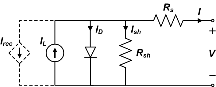
The recombination current $$I_{rec}$$ is governed by:
$${I_{rec}} = {I_L}{{d_i^2} \over {{m_{eff}}\left[ { {N_S} {V_{bi}} – \left( {V + I{R_s}} \right)} \right]}} \qquad$$
Inclusion of this current sink changes the standard single diode equation to:
$$I = I_L \left[ 1 – \frac{d_i^2 / m_{eff}} {N_S V_{bi} – \left( V + I R_s \right)} \right] – I_0 \left[ \exp \left( \frac{V + I R_s} {n N_S V_T} \right) – 1 \right] – \frac{V + I R_s} {R_{sh}} \qquad$$
where $$d_i$$ is the thickness of the intrinsic layer that separates the p and n junctions, $$V_{bi}$$ is the voltage potential across the intrinsic layer, and $$m_{eff}$$ ($$\mu \tau eff$$ in the PVsyst User’s Guide, and $$\mu \tau_{eff}$$ in Mermoud and Lejeune, 2010 ) is the effective diffusion length of the charge carrier. In implementation, $$V_{bi} = \textup{0.9 V}$$ per junction is typical (see PVsyst User’s Guide), and the quantity $$d_i^2/ m_{eff}$$ is combined into a single parameter.
[1] K. J. Sauer, T. Roessler, C. W. Hansen, Modeling the Irradiance and Temperature Dependence of Photovoltaic Modules in PVsyst, J. of Photovoltaics 5(1), Jan. 2015.
Content for this page was contributed by Matthew Boyd (NIST) and Clifford Hansen (Sandia)